
Bug free PCB’s manufactured by ECL.
European Circuits first came into contact with Boldport on Twitter.
We both design electronics and converse about PCBs online, so it now seems like a natural progression that we would eventually get round to discuss working together on a project.
Following discussions, we were delighted to be chosen to manufacture a new version of a badge the company made for a hardware security conference in The Hague.
Boldport founder, Saar Drimer says “I agreed to help out the folks at hardwear.io by designing a simple PCB-based badge for their conference. They suggested a board in a shape of a ladybird, so that’s the direction I took. I knew that the kit needed to be cheap and fun so I worked within those constraints, and so made the components play a significant part of the physical appearance of the final build. It even surprised me with how much character it had when I built the first one.
I’ve now improved the design, and called it ‘The Lady’, which is what ECL manufactured. This project is open source and you can get it from https://github.com/boldport/thelady
The Lady’ is Boldport Club‘s fourth project, which will be sent out to members in June. The Club is a subscription to a monthly delivery of projects that I create. With these projects I aim to encourage experimentation and discovery through electronics, and create things that people haven’t seen or experienced before.
We design electronics with the same attention to functional and aesthetic detail as one would similarly expect from a master woodworker. We call it ‘electronics craftsmanship, and like those serious about their craft, we developed our own custom circuit design tool to allow us to achieve exactly what we want, how we want it. We work with companies that want their electronics unique and distinct, and depart from the typical ‘square and green’ type.”
In what is an aesthetically pleasing piece of design, we decided to take photos of various stages of board’s creation here at the ECL factory.
It is our hope that this article will give the reader a better understanding of the processes and procedures we undertake here to ensure a consistent quality of PCBs being produced, whilst also being informative to those that may not know how a Printed Circuit Board is made.
Making the PCB
At the outset it is important to give us as much information about your board as possible. In the case of “The Lady”, the board specifications were as follows:
- Material Type: FR4.
- Copper Weight: 1oz.
- Legend: White
- Legend Side: Both Sides
- Material Thickness: 1.6mm
- Panel Form or Single Circuits: Single Circuits
- Solder Mask: Red
- Solder Mask: Both Sides
- Surface Finish: Nickel Gold
- Type of Board: PTH
Film Generation

Armed with this information, the first step in the journey of a PCB is taking the Gerber files (supplied by Boldport) and generating a film representation of the board layout. A film is required for each ‘layer’. In the case of “The Lady” we generated film for the copper layers, solder resist and legend.
Test
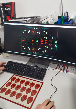
All our bare printed circuit boards are ATE tested for continuity.
Cut Raw Material

We would class a standard PTH board cut to be, double sided, copper clad, FR4 and 1.6mm thick and this this particular board fits into this category. The panel size was 12 x 10 inches, meaning we could fit 18 circuits this time around. There are all sorts of different variations of material cut, please see Bare Board Specification for more information.
Drill Holes
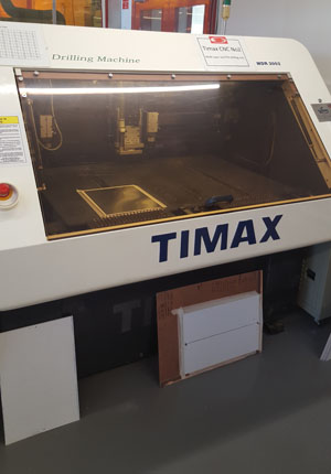
The raw material is then taken to our drill area where we drill the precise hole pattern for the board using NC drill machines.
“The Scrubber”!

Brush scrubbing with pumice has been the industry standard for many years. The use of nylon brushes with a suspension of pumice in water results in excellent surface topography and provides uniform abrasion/polishing. We perform the scrub after every stage of the manufacturing process.
Carbon Application

Next up is the carbon application stage which is an electrochemical process to build up copper in the holes and on the trace area.
Apply Image

At this point we apply photosensitive dry film (plate resist) to the panel. The UV light source and film are used to expose and develop selected areas of the panel.
Pattern Plate

As the name implies, this involves masking off most of the copper surface and plating only the traces and pads of the circuit pattern.
Etch & Strip

We then proceed to removing the dry film and we etch exposed copper.
Test
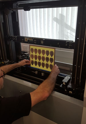
We test the board three times during it’s creation, at the beginning, prior to printing and a final inspection.
Solder Mask
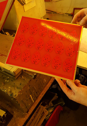
We then take the board and apply the specified red solder mask to the entire board with the exception of the solder pads.
Board Finish

After we apply the solder mask to both sides and it has dried in the oven for 30 minutes. We move onto giving the board its finish. In this case we use Nickel Gold which is slightly more expensive. This is now arguably the most used finish in the PCB industry due the growth and implementation of the RoHs regulation. Nickel Gold provides a flat surface and has a long shelf life too.
We then go back and expose the solder in the photomech room.
Legend
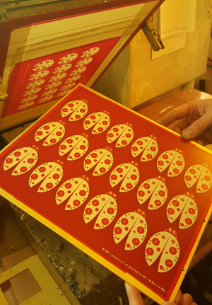
Next up, we apply component idents using a silk screen printing process.
Fabrication
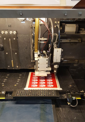
The penultimate step is to route the perimeter of the board using the NC router.
Test

Following on from final test we package and send to the customer.
Contact us today for a Same Day PCB Quotation: Contact Us
